Introduction – Third-Generation Semiconductors: Boom, Bottlenecks, and CIOE's Role
2025 is a landmark year for global advanced manufacturing, with Third-Generation Semiconductors emerging as the backbone of new energy vehicles (NEVs), 5G infrastructure, and grid storage. Silicon carbide (SiC)—the core material for SiC-Based Power Devices—drives this revolution, with the global N-type SiC substrate market set to hit $2 billion. Yet a critical bottleneck persists: high-end wet chemicals for SiC processing face supply chain volatility worldwide, clashing with surging demand for reliable, compliant solutions.
This symbiotic relationship of "opportunities and challenges" rendered the 26th China International Optoelectronic Expo (CIOE 2025) a pivotal event. Held on September 10th in Shenzhen, the 300,000㎡ expo adopted a synergistic "optoelectronics-semiconductor" dual-show paradigm, convening over 3,800 enterprises to showcase Third-Generation Semiconductor breakthroughs—ranging from 8-inch SiC wafers to integrated power modules.
As a provider of high-end industrial cleaning solutions, Shenzhen Yuanan Chemtech's team attended to decode industry signals. What we saw in key clients' booths confirmed: precision (for SiC yield), supply chain resilience (for consistent production), and ESG compliance (for global markets) are non-negotiable. This article explores how our SiC Substrate Micro-particle Cleaner (tailored for Third-Gen Semiconductors) and other solutions align with leaders like TanKeBlue, SICC, Luxshare ICT, and BYD—while delivering actionable insights for advanced manufacturing stakeholders.

Outdoor view of CIOE 2025 venue entrance with clear sky and white clouds.

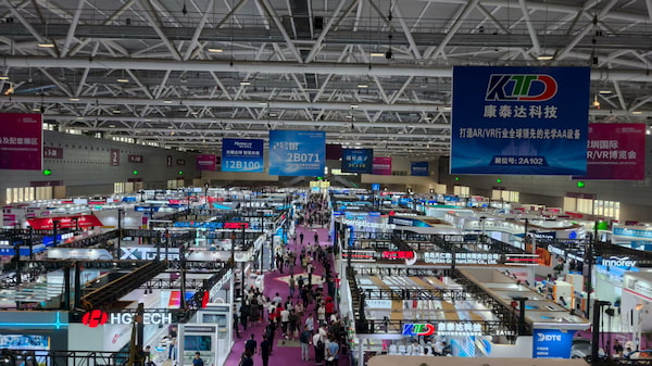
Laser equipment exhibition area in Hall 2.

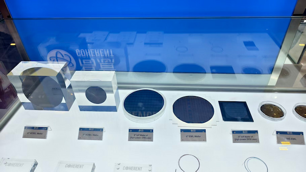
Coherent's booth displaying 3"/6" VCSEL, InP, and EML wafers for lasers.
1. CIOE 2025 Core Client Insights – Needs, Solutions, and Strategic Value
At CIOE 2025, top manufacturers' exhibits revealed clear pain points in advanced manufacturing—especially for Third-Generation Semiconductors. Below is a breakdown of their priorities, how Yuanan's solutions fit, and the tangible value delivered for real-world production:
(1) TanKeBlue (SiC Leader) – High-Precision Cleaning for 6"/8" Wafers in Third-Gen Semiconductors
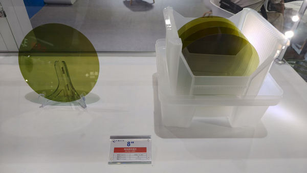
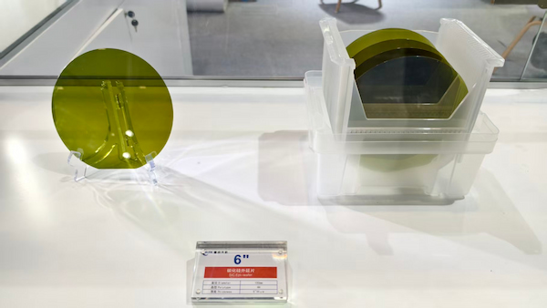
TanKeBlue, a global leading SiC substrate supplier (17.3% global conductive SiC market share, 2024), dominated the semiconductor pavilion with 6-inch and 8-inch SiC epitaxial wafers (marked 4H/6H crystal type, 100-150μm thickness). These wafers are the foundation of SiC-Based Power Devices in NEV traction inverters—an over $4.5 billion market by 2025—and by the middle of 2025, TanKeBlue had accumulatively shipped 1M+ substrates to power global EV brands.

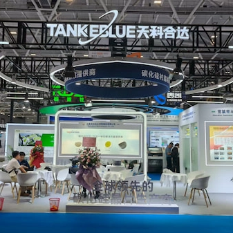
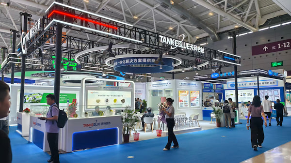
TanKeBlue's exhibition booth at CIOE 2025, focused on SiC materials.

8-inch SiC epitaxial wafer on display at TanKeBlue's CIOE 2025 booth.

6-inch SiC epitaxial wafer exhibited at TanKeBlue's CIOE 2025 stand.
A critical hurdle in TanKeBlue's production line is post-polishing 0.1μm-level micro-particles: even tiny contaminants cause epitaxial layer defects that slash wafer yield. Our SiC Substrate Micro-particle Cleaning Agent resolves this with 99.9% particle removal efficiency and thermal stability, eliminating sub-micron residues without etching or damaging the wafer surface—directly boosting SiC Wafer Defect Control rates. This precision is even more valuable as TanKeBlue scales 8-inch SiC production (backed by its 2025 total capacity plan of near 1 million substrates) to meet global demand: our cleaner seamlessly adapts to 6"/8" wafer sizes without performance loss, supporting its market expansion. And with TanKeBlue producing 75K+ substrates monthly, our 50,000+ ton annual capacity (backed by global logistics partnerships) ensures on-demand delivery that avoids production lags.
(2) SICC – Steady Supply for 8"/12" SiC Substrates (Third-Gen Semiconductor Scalability)
While SICC did not exhibit at CIOE 2025, its role in scaling Third-Generation Semiconductor production globally is irreplaceable. As a top-tier SiC enterprise publicly listed on both the Shanghai and Hong Kong stock exchanges and the world's third-largest substrate manufacturer (17.1% global share, 2024), it leads 8-inch SiC mass production and pioneered 12-inch development—key to lowering SiC-Based Power Device costs for international clients like Infineon and Bosch.
SICC's push for larger wafer sizes brings unique cleaning challenges: 12-inch substrates are more prone to scratch damage and uneven particle adhesion during processing. Our cleaner's low-foam, mild alkaline formula balances aggressive contaminant removal with material compatibility, making it ideal for 8"/12" wafer workflows. For SICC's goal of building a resilient global supply chain, our 18+ years of specialized formulation experience positions us as a trusted partner that meets Third-Generation Semiconductor quality standards worldwide. Supply consistency is equally critical: we maintain dedicated inventory hubs and offer 72-hour emergency response for custom batches, ensuring the 5-10 ton monthly supply needed to keep its global lines running.
(3) Luxshare ICT & Luxvisions Innovation – Wafer Cleaning for Third-Gen Semiconductor Ecosystems
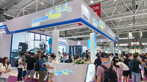
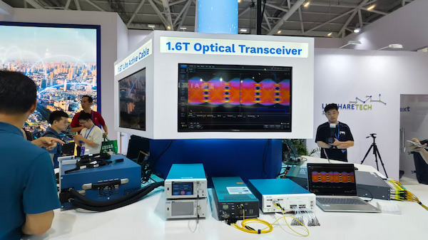
Luxshare ICT and its subsidiary Luxvisions Innovation showcased wafer-level optical modules at CIOE—components that power 5G base stations and NEV sensor systems, both integral to the Third-Generation Semiconductor ecosystem. As core suppliers to Apple and Huawei, they process approximately 150K+ wafers monthly across global facilities, with zero tolerance for quality or supply disruptions.

Luxshare Tech's CIOE 2025 booth with "What's Next" and R&D investment notes.

1.6T Optical Transceiver exhibited at Luxshare Tech's CIOE 2025 stand.
Residual contaminants on optical wafers are a silent risk for their production: even minor residues cause signal interference in 5G modules, leading to costly rework. Our Wafer Cleaner addresses this with ultra-low particle counts (≤0.5 particles/cm²) and fast drying (30s at 80℃), preserving module performance while speeding up processing. For their high-volume commitments to global brands, supply chain resilience is non-negotiable—and our track record of 2+ years of stable cross-regional shipments (with zero disruptions) delivers that reliability. Compliance is another box to check: our cleaner is fully RoHS/REACH-certified, with MSDS documents readily available for audit to meet global brand standards.
(4) BYD – ESG-Compliant Cleaning for NEV Battery & Third-Gen Semiconductor Ecosystems
BYD launched its Chess Plus energy storage system at CIOE, featuring corrosion-resistant battery casings and AI safety monitoring—reflections of its focus on reliability and sustainability for global markets. While BYD integrates SiC-Based Power Devices in its NEVs (boosting energy efficiency by 15%) across global production bases, our collaboration supports its battery manufacturing: a critical link in the NEV supply chain that feeds into the broader Third-Generation Semiconductor ecosystem.
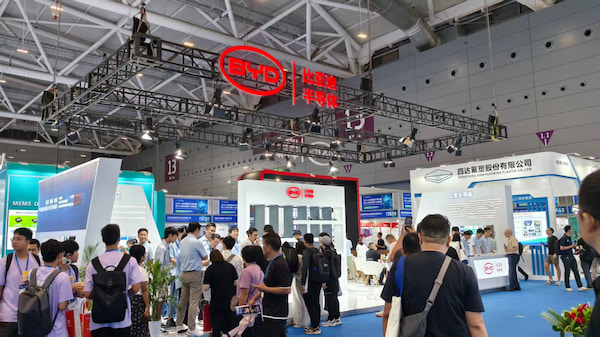
BYD Semiconductor's booth at CIOE 2025, with "Power Semiconductor" signage.
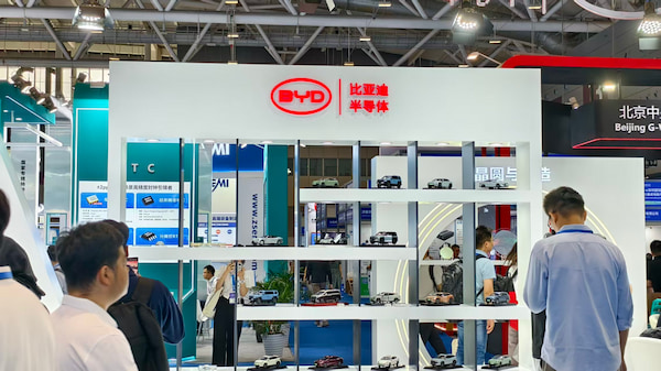
Vehicle model exhibit at BYD Semiconductor's CIOE 2025 booth.

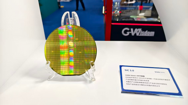
BYD's SiC 3.0 MOS chip (1200V 30mΩ) with self-developed planar gate tech.
Battery shell cleaning residues are a hidden threat to BYD's quality: leftover chemicals cause corrosion that shortens battery lifespan. Our cleaner eliminates this risk with zero-residue performance, passing 500+ hours salt spray tests to ensure casing durability. As BYD expands into European and US EV markets, ESG compliance has become an entry requirement—and our cleaner reduces VOC emissions by 30% compared to industry averages, aligning with its global carbon neutrality goals. For its 2M+ annual NEV battery production worldwide, scalability matters too: our flexible supply model (including IBC ton barrel packaging and regional delivery hubs) matches its distributed production needs.
(5) Goeroptics – Cutting Fluids for Optical Components in Third-Gen Semiconductor Downstream
Goeroptics displayed ultra-lightweight AR/VR smart viewers (75g) at CIOE—devices that rely on precision optical components (lenses, prisms) processed from brittle materials. These tools are increasingly used for Third-Generation Semiconductor factory maintenance and training globally, where visual clarity directly impacts operational efficiency.

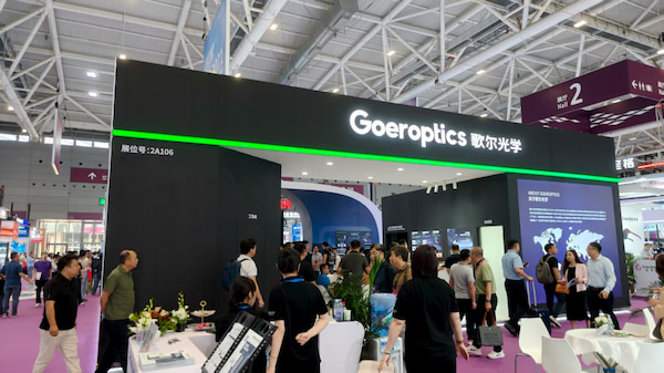
Goeroptics' CIOE 2025 booth (Booth No. 2A106) in the AR/VR zone.

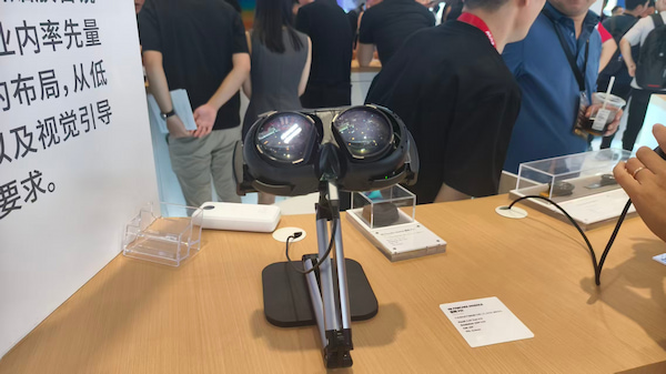
Goeroptics' VR glasses exhibit, labeled as "mass-produced first in industry".

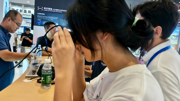
Yuanan Chemtech staff testing Goeroptics' VR glasses at CIOE 2025.
Brittle material cutting (e.g., sapphire) poses a unique challenge: debris buildup scratches surfaces, ruining the 50° FOV with edge-to-edge clarity critical for AR/VR usability. Our Cutting Fluid solves this by improving debris dispersion efficiency by 50% through proprietary polymer dispersants, dropping scratch defects from 5% to less than 0.4% and preserving component precision. For Goeroptics, this precision is a competitive edge in global markets—our fluid's consistent performance supports its "zero-defect component" claim. And with its high-mix, low-volume production across regions, flexible supply is key: we offer 25L to 1000L packaging options and volume-based pricing, keeping small-batch procurement costs manageable worldwide.
To clearly map our clients' core needs to Yuanan's solutions and highlight the value of our offerings, we've summarized the key alignments below:
Partner Client | Core Production Scenario | Critical Cleaning Pain Point | Yuanan Solution | Core Value |
TanKeBlue | 6"/8" SiC epitaxial wafer production | 0.1μm particles causing epitaxial layer defects | SiC Substrate Micro-particle Cleaner | 99.9% particle removal, adapts to Third-Generation Semiconductor large-size wafers, improves SiC Wafer Defect Control |
SICC | 8"/12" SiC substrate mass production | Scratch damage & uneven particle adhesion on large wafers | SiC Substrate Micro-particle Cleaner | Low-foam neutral formula, supports SiC-Based Power Device cost reduction, 5-10 tons monthly stable supply
|
Luxshare / Luxvisions | Wafer-level optical module processing | Residues causing 5G signal interference | Wafer Cleaner | ≤0.5 particles/μm², RoHS-compliant, fits Third-Generation Semiconductor ecosystem supply chains
|
BYD | NEV battery casing manufacturing | Residue-induced corrosion & non-compliant VOC emissions | Eco-Friendly Battery Cleaner
| Zero residue and 30% VOC reduction, enables ESG compliance for Third-Generation Semiconductor downstream
|
Goeroptics | AR/VR optical component cutting | Debris scratches damaging 38° FOV clarity | High-Precision Cutting Fluid | 50% debris settlement efficiency, supports "zero-defect components" for Third-Generation Semiconductor equipment
|
2. Yuanan's Technical Edge – Tailored for Third-Generation Semiconductors & Global Manufacturing
Our solutions tackle three key aspects of advanced manufacturing: scale, precision, and sustainability. We focus on the needs of Third-Generation Semiconductors and global supply requirements. Below is a structured breakdown of our core capabilities:
Technical Dimension | Core Capabilities | Target Application | Keyword Alignment |
SiC-Specific Formulation | Removes 0.1μm particles, thermal stability, compatible with 6"/8"/12" wafers, no etching | Third-Gen Semiconductor SiC substrate/epitaxy | SiC Substrate Micro-particle Cleaner, SiC Wafer Defect Control
|
Global Supply Resilience | 50,000+ ton/year capacity (Dongguan plant), 3-month raw material stock, 72-hour custom response | Multi-regional mass production enterprises | Third-Generation Semiconductors, Supply Chain Stability |
Global Compliance | REACH/RoHS certified, 30% lower VOC emissions, 80% formula recyclability (20% waste reduction) | Export-oriented & high-end manufacturing | ESG, SiC-Based Power Devices, Wet Electronic Chemicals |
3. Key Trends from CIOE 2025 – Implications for Your Cleaning Strategy
CIOE's exhibits and expert forums (featuring PhotonDelta, NSTIC) revealed trends that will shape cleaning needs for Third-Generation Semiconductors and beyond—with actionable takeaways:
(1) 8-Inch SiC Is Non-Negotiable – Upgrade Cleaners Now
8-inch SiC substrates will account for 20% of global production (2025 forecast), but generic cleaners cause 30% higher particle residue compared to specialized cleaners on larger wafers. Action: Prioritize cleaners with size-adaptive formulas (like Yuanan's) to avoid yield losses.
(2) Supply Chain Resilience Is Mandatory – Choose Globally Capable Suppliers
International speakers emphasized "supply chain resilience" to mitigate geopolitical and logistical risks. Action: Partner with suppliers that combine specialized Third-Generation Semiconductor expertise with global delivery capabilities (Yuanan's 60+ patents cover SiC cleaning technology, backed by cross-regional supply networks).
(3) ESG = Market Access – Cleaners Must Be Green
Brands like BYD and Infineon now require suppliers to report chemical VOC emissions globally. Action: Adopt low-VOC, recyclable cleaners (Yuanan's reduce VOCs by 30%) to retain high-value clients.
To connect trends to actionable steps for manufacturers, we've organized the key implications below:
Industry Trend | Core Enterprise Challenge | Practical Action Recommendation | Yuanan Adaptive Solution |
8-inch SiC becomes mainstream (15%-20% of 2025 capacity) | Generic cleaners double defect rates on large wafers | Prioritize size-adaptable specialized cleaners | SiC Substrate Micro-particle Cleaner (6"/8"/12" compatible) |
Supply chain resilience is critical | Imported chemical shortages/delivery delays | Choose suppliers with "technology and supply" dual guarantees | Local capacity and global logistics, 72-hour emergency response |
ESG = global market access | Non-compliant VOC emissions block international clients | Adopt low-VOC, recyclable cleaning solutions | Eco-friendly cleaners (30% VOC reduction, REACH certified) |
Conclusion – Yuanan: Your Global Partner in Third-Generation Semiconductor Success
CIOE 2025 made clear: Third-Generation Semiconductors will define the next decade of global advanced manufacturing—and cleaning solutions are the unsung heroes of yield, scalability, and compliance. Shenzhen Yuanan Chemtech's SiC Substrate Micro-particle Cleaner, wafer cleaners, and cutting fluids are engineered to meet these global demands, with a track record of supporting leaders like TanKeBlue, SICC, and BYD across their production networks.
Ready to optimize your SiC processing, wafer cleaning, or brittle material cutting—wherever your facilities are?
→Contact Us for Yuanan Sic Cleaner MSDS & Request a Free Sample
Frequently Asked Questions (FAQ)
Q1: Which SiC wafer sizes is Yuanan's SiC Substrate Micro-particle Cleaner compatible with?
A: It seamlessly adapts to 6-inch, 8-inch, and 12-inch SiC substrates/epitaxial wafers commonly used in Third-Generation Semiconductors. The formula is optimized for the surface characteristics of different-sized wafers, ensuring 99.9% particle removal while avoiding scratch damage on large wafers. It fully matches the mass production needs of leaders like TanKeBlue and SICC.
Q2: Can Yuanan's cleaners meet yield requirements for SiC-Based Power Devices?
A: Absolutely. 0.1μm-level particles on polished SiC wafers are one of the critical factors of SiC Wafer Defect Control failure. Yuanan's cleaner uses "low surface tension formula + precision impurity removal technology" to reduce particle residue to ≤0.1 particle/μm², directly helping clients increase epitaxial layer yield by 5%-8%. It has been validated in TanKeBlue's 1M+ substrate mass production.
Q3: Can Yuanan's supply chain support mass production for Third-Generation Semiconductor enterprises?
A: We offer end-to-end guarantees. Our Dongguan base has a 50,000+ ton/year capacity and 3-month core raw material stock (direct partnerships with Dow and BASF). Dedicated inventory is reserved for key clients like SICC, enabling "48-hour shipment for regular orders and 72-hour response for custom formulas"—fully meeting semiconductor enterprises' "uninterrupted production" needs.
Q4: Do Yuanan's cleaners comply with ESG standards in European and American markets?
A: The entire product line is REACH and RoHS dual-certified, with 30% lower VOC emissions than the industry average and 80% formula recyclability (reducing waste by 20%). We currently support BYD and Goeroptics in serving European and American clients, and can provide MSDS, compliance test reports, and other audit documents on demand.
Q5: How to confirm if Yuanan's cleaners fit my production process?
A: You can verify compatibility through a "3-step assessment": (1) Provide wafer specifications (size, crystal type), processing stage (post-polishing/pre-epitaxy), and existing pain points; (2) Yuanan issues a customized testing plan; (3) We provide 5L free samples for small-batch validation (with on-site technical guidance) to ensure seamless integration with your existing equipment and processes.


