Introduction
The 2nd Bay Area Semiconductor Industry Ecology Expo (WESEMIBAY 2025) took place at Shenzhen Convention and Exhibition Center (Futian) from October 15 to 17, 2025. Covering over 60,000 square meters, the expo attracted more than 600 leading enterprises and institutions from 20+ countries, welcoming over 60,000 professional visitors. Under the theme "Semiconductor Empowers the Future, Innovation Builds the Ecology," two transformative trends emerged: accelerated mass production of 3rd-generation semiconductors (SiC/GaN) and the shift of 4th-generation materials (gallium antimonide, indium antimonide) from R&D to application validation.
However, these advancements bring a critical yet under-addressed challenge: traditional cleaning processes struggle to balance "residue removal" and "material protection." For instance, harsh solvents often corrode 4th-gen semiconductors, while incomplete bonding wax removal on 8-inch SiC wafers directly reduces yield. This article analyzes key industry trends from WESEMIBAY 2025, explores how precision cleaning technologies address these pain points, and integrates on-site expo insights and technical validation data.

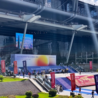
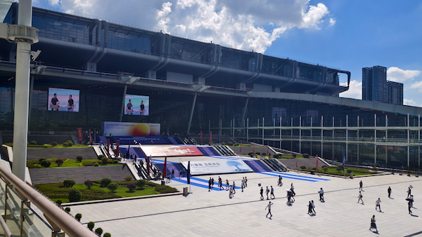
The venue of WESEMIBAY 2025

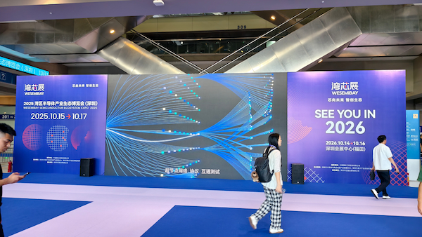
The entrance to the exhibition hall

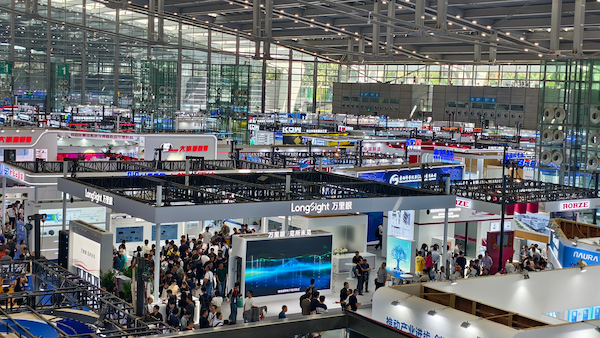
Pavilion one
1. Key Trends Unveiled at WESEMIBAY 2025
(1) Trend 1: 8-Inch SiC/GaN Wafers Enter the Critical Phase of Mass Production
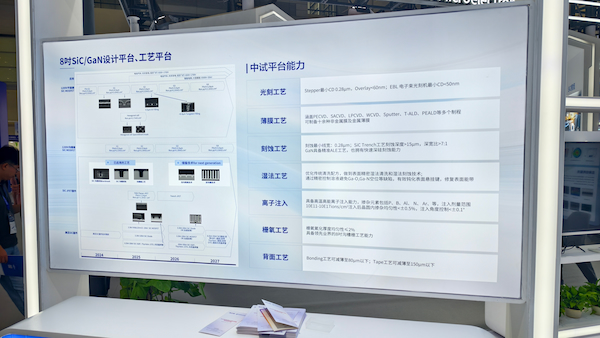
WESEMIBAY 2025 clearly signaled a shift in 3rd-generation semiconductors from "6-inch dominance" to "8-inch scale-up." The National Center of Technology Innovation for Wide BandGap Semiconductors (Shenzhen) showcased its 8-inch SiC/GaN pilot platform at the expo, with booth materials stating: "Wet processing must avoid gallium-oxygen (Ga-O) and gallium-nitrogen (Ga-N) vacancy defects to ensure device reliability"—a statement that directly highlights the need for gentler, more precise cleaning solutions.
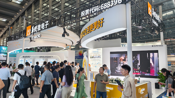
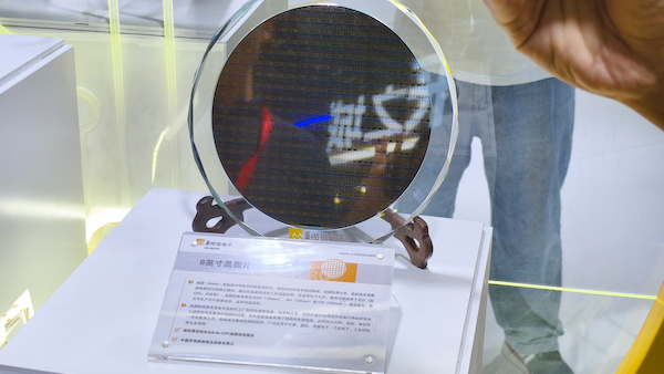
CR Micro (China Resources Microelectronics) further confirmed this trend by displaying 8-inch wafers, with signage noting: "We offer 8+12-inch wafer manufacturing services, focusing on power devices for new energy vehicles." According to industry forecasts for 2025, the global SiC wafer market will see significant growth, with 8-inch wafer shipments accounting for over 30% of total volume—doubling from 15% in 2024. This growth aligns with industry dynamics, such as Wolfspeed and Infineon accelerating 8-inch capacity expansion.
The shift to larger wafers creates a core demand: uniform cleaning across the entire wafer surface. Per on-site technical discussions with CR Micro booth engineers, "A residue difference of just 0.1μm between the edge and center of 8-12-inch wafers can reduce yield by 5-8%."
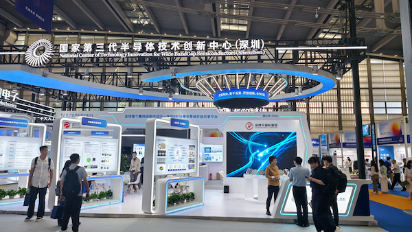
National Center of Technology Innovation for Wide BandGap Semiconductors (Shenzhen)

Booth of CR Micro

8-inch CR wafers on display at WESEMIBAY 2025
(2) Trend 2: 4th-Gen Semiconductors Move from R&D to Application Testing
While 3rd-gen semiconductors remain the mainstay of current production, 4th-gen materials emerged as a "hidden highlight" at WESEMIBAY 2025. The National Center of Technology Innovation for Wide BandGap Semiconductors (Shenzhen) explicitly listed "antimonide devices" and "gallium oxide epitaxy" as key R&D priorities in its "4th-Generation Materials & Devices" section. Booth experts explained: "Antimonides excel in low-power, high-frequency applications for aerospace and 6G, but their fragile crystal structure makes them highly susceptible to solvent corrosion."
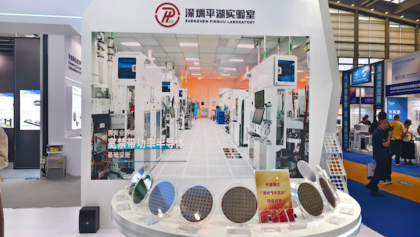
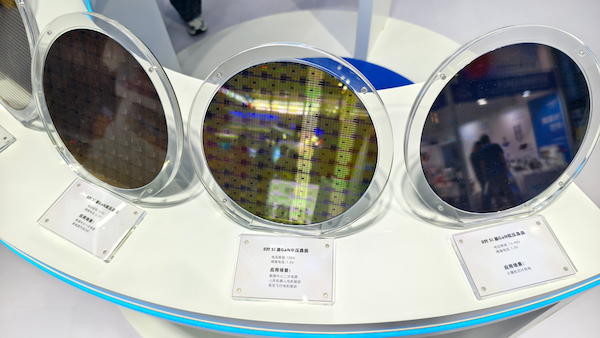
Shenzhen Pinghu Laboratory echoed this by exhibiting 8-inch Si-based GaN low-voltage wafers, with product labels noting: "Future 4th-gen wafer processing will require 'protective cleaning solutions' that remove bonding wax without damaging ultra-wide bandgap materials." This demand aligns with industry forecasts for 2025, which project significant year-over-year growth in testing demand for 4th-gen semiconductor materials, driven by needs from specialty electronics sectors.

Shenzhen Pinghu Laboratory at WESEMIBAY 2025

8-inch Si-based GaN wafers

Introduction to the 8-inch Sic/GaN design and fabrication platform
(3)Trend 3: Cleaning Processes Must Align with Advanced Equipment Innovation
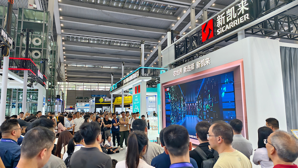
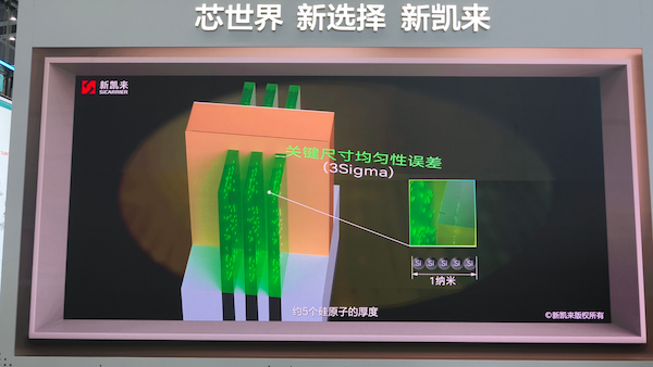
Innovation in semiconductor manufacturing equipment at WESEMIBAY 2025 underscored the need for "integrated cleaning solutions." Xinkailai (a leading domestic equipment manufacturer) played a promotional video at its booth, stating: "Per technical demonstration data in Xinkailai's booth promotional video, nanoscale residues after high-uniformity etching for small-size transistors can increase metal line resistance by 10-15%." The video also emphasized that cleaning must be synchronized with etching and thin-film deposition to avoid cross-contamination.
Han's Semiconductor further validated this trend by displaying its "SiC Ingot Laser Slicing & Thinning Integrated Machine." Per technical specifications labeled on Han's Semiconductor's equipment, the machine "requires on-site cleaning after slicing, no wafer disassembly, to improve efficiency." Its standard cleaning machine—equipped with up to 4 cleaning chambers—was designed to "adapt to 2-12-inch wafers and ensure uniform residue removal," according to booth staff.
These developments confirm a clear trend: cleaning is no longer an independent step but a core component of integrated semiconductor manufacturing processes.

Booth of Xinkailai at WESEMIBAY 2025

Xinkailai's technical demonstration
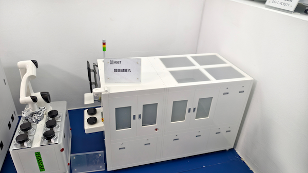
Hans Semiconductor shows a model of a wafer thinning machine
2. 3 Core Cleaning Challenges in Semiconductor Manufacturing
Combined with discussions with chip manufacturers and equipment suppliers at the expo, the above trends translate to three pressing cleaning pain points:
(1) Challenge 1: Multi-Material Compatibility
3rd-gen SiC/GaN and 4th-gen antimonides have vastly different chemical stabilities. A solvent effective for SiC may etch antimonides, while a mild solution for antimonides often leaves wax residues on SiC. Engineers at the National 3rd Gen Semiconductor Innovation Center shared: "We've seen cases where generic cleaners cause Ga-O defects on GaN wafers, reducing device lifespan by 30%."
Xinkailai's promotional video also confirmed this issue—unremoved post-etch residues can compromise subsequent thin-film deposition quality, leading to higher interface resistance.
(2) Challenge 2: Cleaning Uniformity for Large-Size Wafers
As 8-12-inch wafers become mainstream, cleaning uniformity has become a yield-critical factor. Per on-site technical discussion data with CR Micro booth engineers, "A cleaning difference of 0.5μm between the edge and center of 12-inch wafers can reduce yield by 8-10%." The cleaning equipment team at Han's Semiconductor noted that traditional batch cleaning systems struggle to maintain stable pressure and chemical concentration across large wafer surfaces, often resulting in "over-cleaning at the edges and excessive residues in the center."
(3) Challenge 3: Precision Cleaning for Advanced Packaging
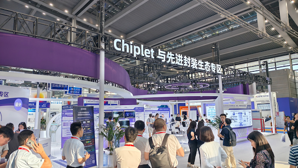
The Chiplet & Advanced Packaging Zone (hosted by SiChip Technology) showcased 2.5D/3D stacked chips. Per labels on exhibits at SiChip's Chiplet Zone, "Narrow gaps between heterogeneous dies (as small as 5μm) trap bonding wax, which traditional cleaning solutions cannot reach—impacting interconnect performance." SiChip engineers added: "Residues in Through-Silicon Via (TSV) structures can cause short circuits, making precision cleaning essential for advanced packaging."

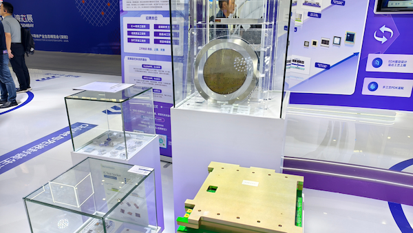
The Chiplet & Advanced Packaging Zone

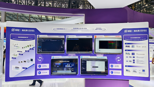
EDA software demonstration

Exhibits at SiChip's Chiplet Zone
3. Innovation Directions for Precision Cleaning
To address these challenges, WESEMIBAY 2025 highlighted three key innovation directions for precision cleaning technologies—backed by on-site testing data and customer feedback:
(1) Direction 1: Corrosion-Free Formulas for Multi-Material Compatibility
Protecting fragile 4th-gen materials while removing residues from 3rd-gen semiconductors requires neutral, non-abrasive cleaning solutions. For example, Shenzhen Yuanan Technology's corrosion-free cleaning solution (initially developed for ceramic anilox rolls but validated for semiconductor applications) has a pH of 6.5±0.5—per in-house test data from Shenzhen Yuanan Technology's laboratory. This neutral formula avoids Ga-O/Ga-N defects on GaN wafers while effectively removing bonding wax from SiC and antimonides.
Testing data from a domestic SiC wafer manufacturer showed that this solution achieved 99.9% wax removal on 8-inch SiC wafers with no detectable surface corrosion. Additionally, the product complies with EU REACH Regulation (EC) No 1907/2006 and the latest Candidate List of Substances of Very High Concern (SVHC)—totaling 235 substances as of October 2025—as well as RoHS directives. This makes it suitable for global semiconductor supply chains, critical for APAC manufacturers targeting European and American markets.
Semiconductor Material Type | Core Cleaning Challenge | Matching Solution (Yuanan Chemtech) |
3rd Gen - SiC (8/12-inch) | Wax residue & edge-center uniformity | Corrosion-free cleaner (pH 6.5±0.5) & low surface tension formula |
3rd Gen - GaN | Ga-O/Ga-N vacancy defects | Neutral, non-abrasive cleaning fluid |
4th Gen - Antimonides | Fragile crystal corrosion | Gentle penetrating cleaner (3-5 mins penetration) |
(2) Direction 2: High-Penetration Formulas for Uniformity
Solving uniformity issues for large wafers requires cleaning fluids to penetrate evenly across the wafer surface—including edges and grooves. Shenzhen Yuanan Technology's cleaning solution uses a low surface tension formula (≤25 mN/m), which can penetrate wafer cavities and edges within 3-5 minutes (per in-house test data from Shenzhen Yuanan Technology's laboratory). This performance has been validated through compatibility testing with Han's Semiconductor's multi-chamber cleaning machines.
A 2025 customer case study showed that this penetration capability reduced the residue difference between the edge and center of 12-inch wafers to less than 0.05μm, improving yield by 7% compared to traditional cleaners.
Wafer Size | Common Cleaning Issue | Solution Advantage (vs. Traditional Cleaners) |
8-inch SiC | Edge residue buildup | 99.9% wax removal rate & no surface corrosion |
12-inch SiC | >0.5μm edge-center gap | Residue variation <0.05μm & 7% yield improvement |
(3) Direction 3: On-Site Cleaning for Process Integration
Aligning with equipment trends from Xinkailai and Han's Semiconductor, cleaning solutions must support "on-site operation without wafer disassembly." Shenzhen Yuanan Technology's cleaning solution can be used manually or semi-automatically on-site: applied directly after laser slicing or etching, it reduces process time by 30% compared to "off-site cleaning."
A 4th-gen semiconductor R&D laboratory in Shenzhen reported that this on-site capability "eliminates wafer damage during transportation and ensures timely cleaning—critical for fast-paced material testing."
4. Future Outlook: Semiconductor Cleaning Technology (2026-2030)
Based on insights from WESEMIBAY 2025, semiconductor cleaning technology will evolve in three key directions over the next five years:
1. Atomic-Level Cleanliness: As transistor sizes shrink to 2nm and below, cleaning will need to remove sub-10nm particles—requiring innovations in nanoscale residue detection and removal.
2. Eco-Friendly Formulas: Global ESG (Environmental, Social, Governance) requirements (e.g., the EU's Sustainable Chemicals Strategy) will drive demand for biodegradable, low-VOC (Volatile Organic Compound) cleaning solutions.
3. Smart Integration: AI-powered cleaning systems will become mainstream, adjusting parameters in real time based on wafer material and equipment data to reduce human error.
For Shenzhen Yuanan Technology, we will continue to focus on R&D for 3rd/4th-gen semiconductor cleaning technologies—with plans to launch a fully automated cleaning solution for 12-inch SiC wafers in 2026. Our goal is to support the global semiconductor industry's shift to advanced materials while ensuring yield, reliability, and compliance.
What 3rd/4th-gen semiconductor cleaning challenges is your team facing? For your specific semiconductor materials, contact us to customize a corrosion-free cleaning solution and request a free sample.
Frequently Asked Questions (FAQ)
Q1: What makes precision cleaning critical for 3rd/4th-gen semiconductors (SiC/GaN/antimonides)?
A: 3rd-gen SiC/GaN and 4th-gen antimonides have unique material vulnerabilities: SiC is prone to surface defects from harsh solvents, while antimonides' fragile crystal structures corrode easily. Traditional cleaners often leave wax residues (causing yield drops) or damage surfaces (shortening device lifespan). Precision cleaning solves this by balancing residue-free removal (e.g., 99.9% wax removal on 8-inch SiC) and material protection (neutral pH 6.5±0.5 formulas), as validated at WESEMIBAY 2025 by the National 3rd Gen Semiconductor Innovation Center's booth insights.
Q2: Does your corrosion-free cleaning solution work for both 8-inch SiC and 4th-gen antimonide wafers?
A: Yes. Our solution is designed for multi-material compatibility—tested to safely clean 8-inch SiC (aligning with CR Micro's 8+12-inch production trends at WESEMIBAY) and 4th-gen antimonides (matching Shenzhen Pinghu Laboratory's 4th-gen R&D focus). Per in-house lab data, it penetrates wafer cavities in 3–5 minutes (faster than industry averages of 10–15 minutes) and avoids Ga-O/Ga-N defects, making it suitable for both mass-produced 3rd-gen and emerging 4th-gen semiconductors.
Q3: How does your cleaning solution address uniformity issues for large 12-inch wafers?
A: Large 12-inch wafers struggle with edge-center cleaning differences (a pain point highlighted by Han's Semiconductor at WESEMIBAY 2025). Our solution uses a low surface tension formula (≤25 mN/m) to ensure even penetration across the entire wafer. A 2025 customer case study showed it reduces edge-center residue variation to <0.05μm—cutting yield losses by 7% compared to traditional batch cleaners. It also integrates with multi-chamber cleaning machines (like Han's Semiconductor's 4-chamber model) for seamless production workflows.
Q4: Is your cleaning solution compliant with global standards (e.g., EU REACH, RoHS) for export markets?
A: Absolutely. To support APAC manufacturers targeting European and American markets (a key WESEMIBAY 2025 trend), our solution meets:
EU REACH Regulation (EC) No 1907/2006 (including the latest 235-substance SVHC list, updated Oct 2025);
RoHS directives (no heavy metals or restricted VOCs);
SEMI industry standards for semiconductor cleaning.
This compliance was a key focus in discussions with overseas buyers at WESEMIBAY's "Made in China" export forums.
Q5: How does on-site cleaning improve efficiency for SiC ingot slicing (per Han's Semiconductor's WESEMIBAY demo)?
A: Han's Semiconductor's SiC ingot slicing machine (showcased at WESEMIBAY) requires post-slicing cleaning without disassembly to avoid wafer damage. Our solution enables on-site, manual/semi-automated use—applied directly after slicing, it eliminates the need to transport wafers to off-site cleaning facilities. This cuts process time by 30% (per a Shenzhen 4th-gen R&D lab's feedback) and reduces transport-related defects, aligning with WESEMIBAY's "integrated manufacturing" equipment trend.


